Tue, Jan 21, 2025
[Archive]
Volume 20, Issue 2 (June 2023)
IJMSE 2023, 20(2): 1-24 |
Back to browse issues page
Download citation:
BibTeX | RIS | EndNote | Medlars | ProCite | Reference Manager | RefWorks
Send citation to:


BibTeX | RIS | EndNote | Medlars | ProCite | Reference Manager | RefWorks
Send citation to:
Molaei M J. Light-Emitting Diodes Based on Van Der Waals Heterostructures: a Review. IJMSE 2023; 20 (2) :1-24
URL: http://ijmse.iust.ac.ir/article-1-3019-en.html
URL: http://ijmse.iust.ac.ir/article-1-3019-en.html
Abstract: (8344 Views)
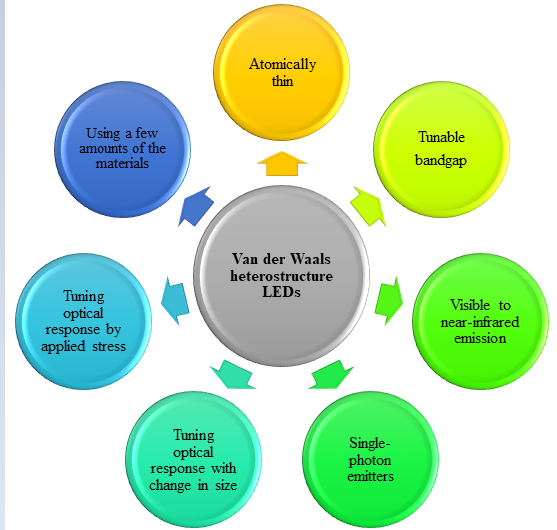
The introduction of the 2D materials in recent years has resulted in an emerging type of the constructed structures called van der Waals heterostructures (vdWHs) that take advantage of the 2D materials in forming atomically thin components and devices. The vdWHs are constructed by the stacking of 2D materials by van der Waals interactions or edge covalent boning. The electron orbitals of the 2D layers in vdWHs extend to each other and influence the electronic band structures of the constituent layers. The tunable optical response over a wide range of the wavelengths (NIR to visible) can be obtained by assembling vdWHs through combining of the monolayers. By application of 2D layers in vdWHs, p-n heterojunctions without lattice mismatch can be formed. The photodiodes based on the van der Waals interactions could be considered as promising candidates for future optoelectronic devices. Furthermore, on-chip quantum optoelectronics can move to the next generation by using 2D materials in vdWHs. In this review, the vdWHs are introduced and their properties and applications in light-emitting diodes (LEDs) have been discussed. The vdWHs allow bandgap engineering, and hence, LEDs working in a range of the wavelengths can be realized. The applications of vdWHs in forming atomically thin components in optoelectronic devices and LEDs have been addressed.
Keywords: Van der Waals heterostructures, 2D materials, band structure, bandgap tuning, light-emitting diode
Type of Study: Review Paper |
Subject:
Casting and Solidification
Send email to the article author
| Rights and permissions | |
 |
This work is licensed under a Creative Commons Attribution-NonCommercial 4.0 International License. |


